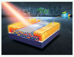
ACS Nano 最新综述:二维与三维材料之间的联系
本综述通过介绍在石墨烯上的金属,金属与二维半导体的联系,石墨烯与传统半导体的联系,二维半导体与传统半导体的联系等阐述了二维和三维材料的关系与展望。
Contacts between Two- and Three-Dimensional Materials: Ohmic, Schottky, and p − n Heterojunctions 共25页 引文176篇
Yang Xu,* ,†,‡,⊥ Cheng Cheng,†,⊥ Sichao Du,† Jianyi Yang,† Bin Yu,† Jack Luo,† Wenyan Yin,† Erping Li,† Shurong Dong,† Peide Ye,§ and Xiangfeng Duan‡
†College of Information Science and Electronic Engineering, Zhejiang University, Hangzhou, Zhejiang 310027, China
‡Department of Chemistry and Biochemistry, University of California, Los Angeles, California 90095, United States
§School of Electrical and Computer Engineering, Purdue University, West Lafayette, Indiana 47906, United States
ABSTRACT: After a decade of intensive research on two-dimensional (2D) materials inspired by the discovery of graphene, the fi eld of 2D electronics has reached a stage with booming materials and device architectures. However, the e ffi cient integration of 2D functional layers with three-dimensional (3D) systems remains a signi fi cant challenge,limiting device performance and circuit design. In this review, we investigate the experimental e ff orts in interfacing 2D layers with 3D materials and analyze the properties of the heterojunctions formed between them. The contact resistivity of metal on graphene and related 2D materials deserves special attention, while the Schottky junctions formed between metal/2D semiconductor or graphene/3D semiconductor call for careful reconsideration of the physical models describing the junction behavior. The combination of 2D and 3D semiconductors presents a form of p−n junctions that have just marked their debut. For each type of the heterojunctions, the potential applications are reviewed brie fl y.期待大家的好评,谢谢!


 京公网安备 11010802022153号
顶一下,感谢分享!
顶一下,感谢分享!
顶一下,感谢分享!
,
牛
段镶峰作品
顶一下,感谢分享!